

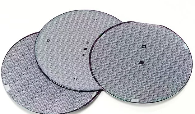
Achieving the correct wafer thickness before assembly is critical in semiconductor manufacturing. Wafer back grinding (or wafer thinning) is a semiconductor manufacturing process designed to control the wafer thickness, which is essential to produce ultra-thin wafers used to create stacked and high-density packaging in compact electronic devices.
Wafer thinning is always a critical process. The chips are already present on the wafer and any failure in the process affects the production yield and costs. Tight in-line control on the thinning in-process operation is possible using contact gauges or non-contact sensors, even in the presence of DI water. Our offering of sensors helps in obtaining a repetitive final thickness of the wafer during the time.
The thinning operation is usually performed in two steps: rough grinding and finish grinding. The first one is used to remove most of the silicon amount during the finish operation just a small amount is removed till the desired final thickness that is normally less than 100µm. Willrich Precision offers a contact gage that can easily control the rough thinning phase and because of its robust design, can survive in DI water without adding unwanted contaminants that could be dangerous to the wafer.
The same is for our offering of non-contact gauges that are particularly useful in the finish phase where particular care has to be taken in order not to damage the wafer.
Willrich Precision is able to supply different gaging solutions to check the thickness of silicon, sapphire, SiC or any other material wafer used in the semiconductor industry. We have gaging systems that control the wire bonding dimension during the drawing process too. Are also available a collection of sensors that are installed on machine tools to measure the physical quantities that affect and govern the machining processes.
Grinding evenly
After sawing the wafers are thinned using mechanical processes such as grinding and lapping. During the grinding of a raw wafer or structured wafer certain quality parameters must be maintained. For raw wafers, for example, the TTV value indicates uniform removal during grinding. The TTV value is statistical value based on a metrological wafer thickness measurement indicating the absolute thickness variation of the entire wafer. The point here is to determine the maximum difference between the thickest and thinnest point, the so-called Total Thickness Variation (TTV).
In the thin wafer polishing process, a polishing pad applies pressure to make contact with the wafer surface and polishes it. A polishing paste (slurry) containing chemically effective substances and abrasive materials are used. The removal on the wafer surface occurs by friction. In a dry-polish process, the chemical and abrasive material is bound in a pad. In this process, a lower contact pressure is sufficient. Optical measuring systems are used for the monitoring of the polishing process, because the determination of the roughness allows conclusions to be made about the surface quality.
Smooth polishing
In the thin wafer polishing process, a polishing pad applies pressure to make contact with the wafer surface and polishes it. A polishing paste (slurry) containing chemically effective substances and abrasive materials are used. The removal on the wafer surface occurs by friction. In a dry-polish process, the chemical and abrasive material is bound in a pad. In this process, a lower contact pressure is sufficient. Optical measuring systems are used for the monitoring of the polishing process, because the determination of the roughness allows conclusions to be made about the surface quality.
It has to be flat: The perfect wafer
The surface finish of the wafer is characterized by its flatness. The flatter the surface, the more perfect the wafer is. Differences in height may lead to contacting problems during subsequent stacking to a 3D IC wafer package.
In addition, the wafers must be ground to an exact thickness and the doping introduced into the substrate should not be removed too far. The wafer edge can also be checked at random with a 2D profile measurement. From this, the wafer manufacturer can determine the wear of the grinding tools and optimize the process parameters. Waste at the edge of the wafer also plays an important role. The more efficiently this is done, the more microchips can be produced on the wafer later and the so-called fill factor increases. Processed wafers that are equipped with bump structures or solder balls, for example, can be measured in terms of height, width and coplanarity.
Willrich Precision offers many different gaging solutions to achieve wafer flatness measurement and wafer thickness measurement